CG MATERIAL
Sapphire Epitaxial Wafer (EPI Wafer)
Sapphire Epitaxial Wafer (EPI Wafer)
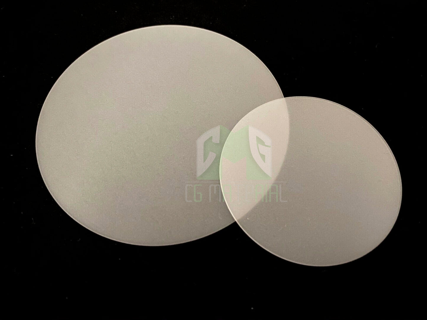
A sapphire epitaxial wafer (EPI wafer) is a type of semiconductor substrate used in the production of electronic devices such as LEDs, lasers, and power electronics. It is made from a single crystal of sapphire grown using a process known as epitaxy, in which a thin layer of a different material is deposited on the surface of the crystal to create a high-quality, single-crystal substrate.
The sapphire EPI wafer is characterized by its high thermal conductivity, chemical stability, and excellent electrical insulation properties. These properties make it ideal for use in high-temperature and high-power applications, as well as in harsh environments that require a high degree of reliability.
The epitaxial layer grown on the sapphire substrate can be made from a variety of materials, including gallium nitride (GaN), aluminum gallium nitride (AlGaN), and indium gallium nitride (InGaN). These materials are used to create different types of electronic devices with specific performance characteristics, such as blue and green LEDs, high-power RF devices, and high-voltage power electronics.
The sapphire EPI wafer is manufactured using advanced crystal growth and processing techniques to ensure the highest possible quality and consistency. These wafers are available in a range of sizes and thicknesses to meet the specific requirements of different applications.
Overall, sapphire epitaxial wafers are an essential component in the production of high-performance electronic devices. Their unique properties make them well-suited for a range of applications in the electronics industry, from lighting and displays to power electronics and advanced communications systems.
| Catalog No. | CERAMICS |
|---|---|
| Size | Customized |
| Material | Al2O3 |
| Purity | 95% 99% 99.7% |
| Density | 3.8~3.9 g/cm3 |
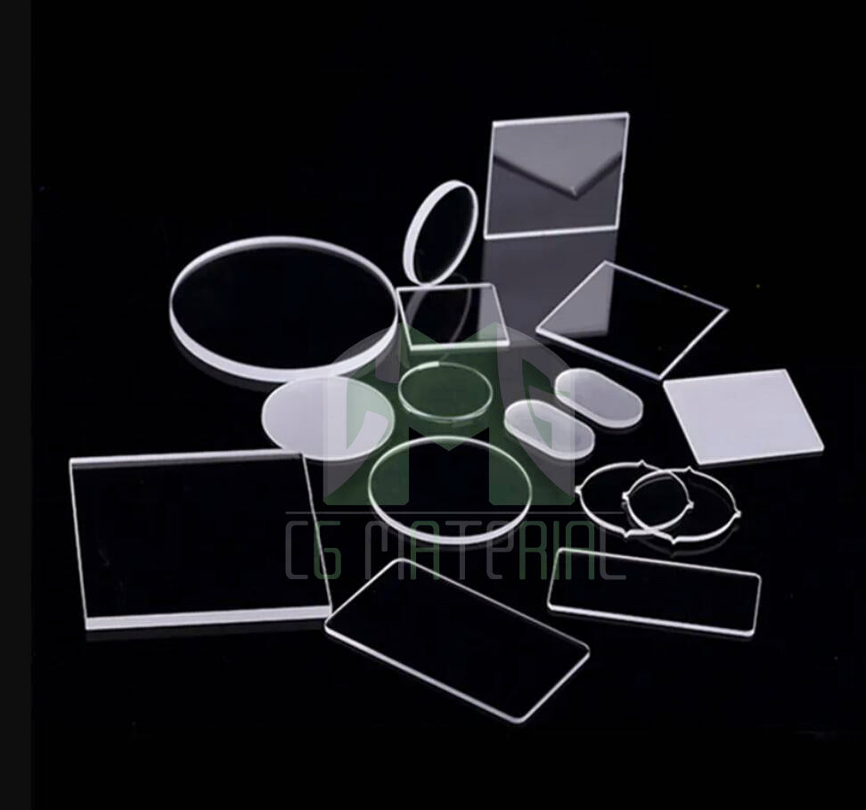
At CG Material, we offer high quality Sapphire Epitaxial Wafer (EPI Wafer) with exceptional purity and precision in terms of size. Our products range in diameter from 1mm to 100mm and have a purity level of up to 99.8%. We also provide custom manufacturing options for special shapes to meet specific needs.
Sapphire Epitaxial Wafer Specifications
| Parameters range for Silicon on Sapphire (SOS) Epi Wafers | |
| Wafer diameter | 76 mm, 100 mm, 150 mm |
| Orientation | (1012) ± 1º (R-plane) |
| Epi-layer thickness, µm | 0.3-2.0 |
| Epi-layer dopant | Phosphorous, Boron |
| n-type | according to spec. |
| p-type | 1,0 – 0,01 |
| Cleaning/packaging |
Class 100 clean room cleaning, vacuum packaging 25 pieces in one cassette packaging or individual packaging. |
Sapphire Epitaxial Wafer Applications
Used as the substrate for the growth of III-V compounds such as GaN for LED's.
Used in aerospace and military applications
Packaging
We handle our products with care to ensure they remain in their original condition during storage and transportation and to preserve their quality.


